SSD NAND Spec Notes
04_20210916_b47r_fortis_512gb_nand_datasheet_Ver.L.pdf
General Description
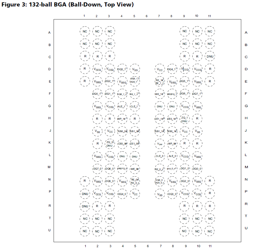
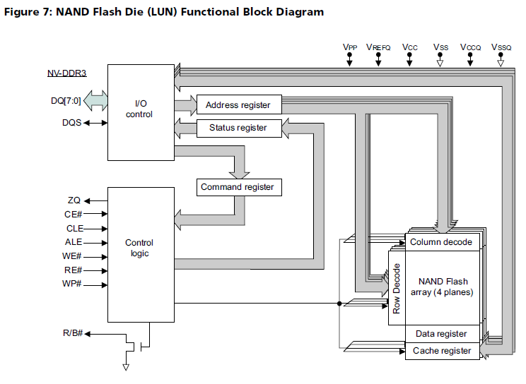
- I/Os transfer commands, address, and data: DQx
- five control signals: CE#, CLE, ALE, WE#, and RE#.
- control hardware write protection: WP#
- monitor device status: R/B#
- bidirectional data strobe: DQS
| Signal | Type | Description |
|---|---|---|
| ALE | Input | Address latch enable: Loads an address from DQx into the address register. |
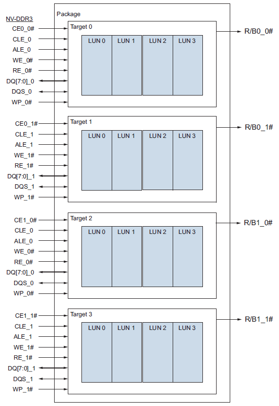
| CE# | Input | Chip enable: Enables or disables one or more die (LUNs) in a target. |
| CLE | Input | Command latch enable: Loads a command from DQx into the command register. |
| DQx | I/O | Data inputs/outputs: The bidirectional I/Os transfer address, data, and command information. |
| DQS, DQS_t | I/O | Data strobe: Provides a synchronous reference for data input and output. |
| DQS_c | I/O | Data strobe complement: Provides a complementary signal to the data strobe signal optionally used for reference for data input and output. |
| RE#, RE_t | Input | Read enable: RE# transfers serial data from the NAND Flash to the host system. |
| RE_c | Input | Read enable complement: Provides a complementary signal to the read enable signal optionally used for reference for data output. |
| WE# | Input | Write enable: WE# transfers commands, addresses. |
| WP# | Input | Write protect: Enables or disables array PROGRAM and ERASE operations. |
| R/B# | Output | Ready/busy: An open-drain, active-low output that requires an external pull-up resistor. This signal indicates target array activity. |
| Vcc | Supply | Vcc: Core power supply |
| Vccq | Supply | Vccq: I/O power supply |
| Vpp | Supply | Vpp: The VPP signal is an optional external high voltage power supply to the device. This high voltage power supply may be used to enhance operations (for example, improved power efficiency). If VPP will not be utilized by a host system, that VPP signal location is then defined as a DNU signal location. |
| Vss | Supply | Vss: Core ground connection |
| Vssq | Supply | Vssq: I/O ground connection |
| Vrefq | Supply | Vrefq: Reference voltage |
| ZQ | - | Reference pin for ZQ calibration: This is used on ZQ calibration. The ZQ signal shall be connected to Vss through RZQ resistor. |
| NC | - | No connect: NCs are not internally connected. They can be driven or left unconnected. |
| DNU | - | Do not use: DNUs must be left unconnected. |
| RFU | - | Reserved for future use: RFUs must be left unconnected. |
Notes: 1. See Device and Array Organization and Signal Assignment sections for detailed signal connections.
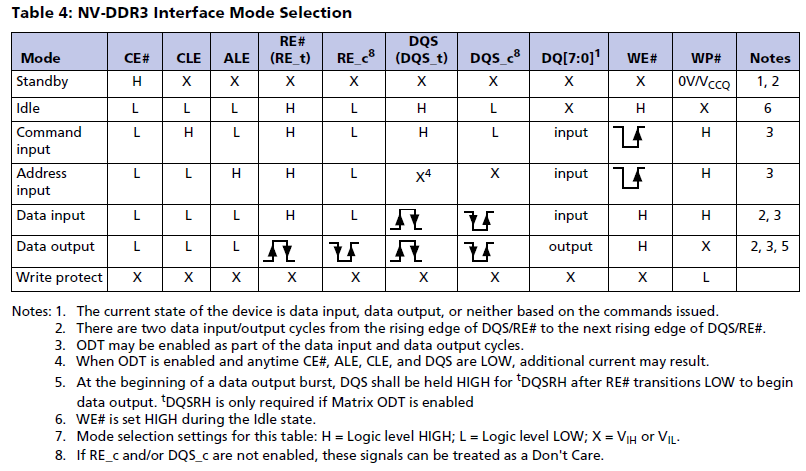
- See Bus Operation – NV-DDR3 Interface for detailed signal descriptions.
Architecture
Bus Operation – NV-DDR3 Interface
Differential Signaling
Warmup Cycles
Warmup Cycle Restrictions
On-Die Termination
Self-Termination On-Die Termination
Concept
Copyback operations: Copyback操作是指将一个页的数据直接拷贝到同一块内的另一个页,无需先将数据读取到外部主存储器的缓冲区,可减少数据传输时间,提高编程效率和系统整体性能。
